Semiconductor Device Pad Printing Packaging Machine, (semiconductor Ic Device Marking and Taping Integrated Packaging Machine)
 - SolidWorks - Free Download")
 - SolidWorks - Free Download")
 - SolidWorks - Free Download")
 - SolidWorks - Free Download")
 - SolidWorks - Free Download")
3D Model of Semiconductor Device Pad Printing and Packaging Machine SW Design Source File Sharing.
The development of pad printing machines towards automation is a consensus in the industry. It is a necessary path to enhance production efficiency and reduce costs, and it is also an inevitable requirement for transforming pad printing technology from a labor-intensive industry to a technology-intensive industry.
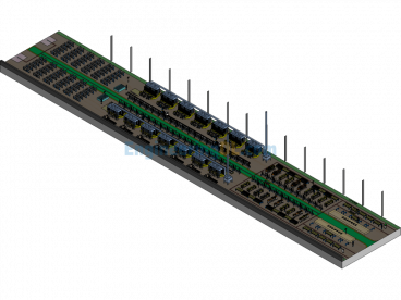
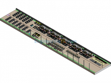
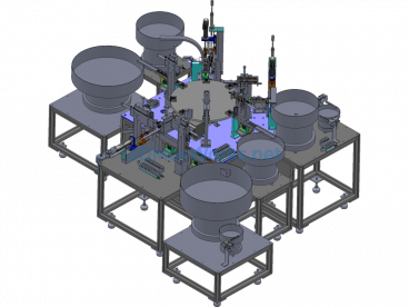
This equipment is an integrated machine for printing, taping, and packaging semiconductor IC devices. The IC device size is very small at 56mm, requiring high precision from the equipment! The design mechanism of this equipment is mature and has significant reference value, containing editable parameters, which is very helpful for designers to learn from! The equipment uses gear step feeding, carrier tape movement, and a robotic arm to grab products for placement in the carrier tape to complete packaging. The model is assembled from components like a hot press feeding mechanism, table, oven, and receiving mechanism, creating a realistic effect. Welcome to download.
Specification: Semiconductor Device Pad Printing Packaging Machine, (semiconductor Ic Device Marking and Taping Integrated Packaging Machine)
|
User Reviews
Be the first to review “Semiconductor Device Pad Printing Packaging Machine, (semiconductor Ic Device Marking and Taping Integrated Packaging Machine)”
You must be logged in to post a review.


There are no reviews yet.